introduce
Complementary Metal Oxide Semiconductor (CMOS) sensors are a technology that has been around since the 1990s. Early CMOS cameras were competing with the more mature CCD technology, but during the 1990s and early 2000s, CMOS sensor technology improved and CCD technology was surpassed as the sensor of choice for consumer digital cameras. The technology was subsequently further improved to meet the higher requirements necessary for scientific imaging.
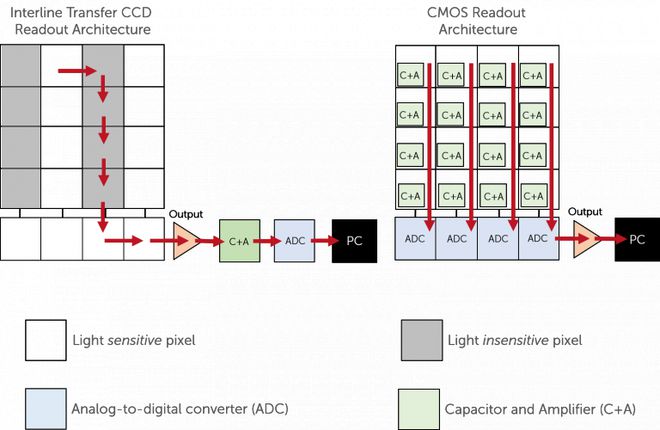
CMOS sensor technology differs from CCD sensors in that, instead of feeding all sensor pixels through one output node, one amplifier, and one analog-to-digital converter (ADC) as in CCD sensors, CMOS sensors have a miniaturized capacitor and amplifier on each pixel, and one ADC on each column (as shown in Figure 1). Each ADC works simultaneously, reading out the entire column, rather than a single pixel of the entire sensor. This makes the process faster and requires 100 times less power than the CCD sensor architecture.

Figure 1: Comparing the readout architectures of interline transfer CCD and sCMOS sensors. Left: Interline transfer CCD format, where electrons are transferred from the sensor to a readout register, to an output node, amplified (via a capacitor (C) and amplifier (A)), and converted to digital grayscale levels by an ADC. This is then sent to a computer. Right: A typical CMOS format, where each pixel has a capacitor and amplifier. This means that photons that hit each pixel create electrons that are converted to a readable voltage across the pixel. The voltages from the entire column are sent to an ADC (of which there is one per column), which is sent directly to a computer. This allows CMOS cameras to be much faster as they work in parallel.
sCMOS Technology
In 2009, scientific CMOS (sCMOS) technology was introduced, and sCMOS cameras became available in 2010-11. sCMOS cameras offer low noise, high speed, and a large field of view, making them ideal for a wide range of applications from astronomy to microscopy.
Rolling Shutter and Global Mode
sCMOS sensors differ from CCD sensors in that they typically have a rolling shutter. Image acquisition starts at the top of the sensor and works its way down line by line. This allows the sensor to acquire images at higher frame rates and with lower read noise. The speed of an sCMOS camera is directly related to the number of lines and the line time, which is the time between acquiring one line and another.
The rolling shutter "opens" and "closes" by clearing the charge already within a row and measuring any new incoming photons. This allows overlap to occur between the current row of pixels in the acquired frame (the image being acquired) and the lower row of pixels in the previous frame (the image being read out) (Figure 2).

Figure 2: Schematic diagram indicating how the acquisition of a frame overlaps with the readout of the previous frame. This enables sCMOS to have fast acquisition and readout.
Some sCMOS sensors can be used in a pseudo-global shutter mode to achieve zero distortion and enable applications involving hardware changes between frames, such as sequential dual-channel acquisition. This pseudo-global shutter takes advantage of the control of the light source triggering. To create this global shutter, the camera needs to activate the rolling shutter in dark conditions. Then, by triggering the light source and stopping the light at the same time as stopping the camera, an area of the array can be illuminated at the same time, just like a global shutter (as shown in Figure 3).

Figure 3: The three main shutter formats. Most CCD/EMCCs have a true global shutter, which allows all pixels to be read simultaneously when they are exposed to light. Most sCMOS sensors have a rolling shutter, which, while fast and sensitive (from a back-illuminated sensor), can produce artifacts. A pseudo-global shutter uses a trigger to control the light source, allowing a global shutter to be used within a rolling shutter (if timed precisely).
Comparison between CCD and sCMOS
The differences in CCD and sCMOS sensor architectures have both advantages and disadvantages. Some of the advantages of sCMOS technology over CCD technology are as follows:
1. Low read noise: sCMOS has a read noise of ~1 e-, while CCD has a read noise of 5-6 e-. To learn about the role of reduced read noise and increased sensitivity, click here.
2. High speed: sCMOS can reach up to 100s fps, while CCD is ~20 fps. This is because each column has an associated ADC, so a small portion of the data needs to be processed.
3. Large field of view: sCMOS sensors have a diagonal range of 19-29 mm, while CCDs have a diagonal range of 11-16 mm
4. Power efficiency: Due to parallelization, sCMOS consumes 100 times less power than CCD
While sCMOS technology is superior to CCD technology in many ways, it does have some disadvantages:
Increased temporal and fixed pattern noise: When each pixel is read out individually, more temporal and fixed pattern noise is introduced. sCMOS sensors have more active readout area compared to CCDs, which leads to an increase in these noise sources. This can be reduced by careful electronic design and calibration by the camera company.
Rolling shutter artifacts: sCMOS sensors can use a rolling shutter to acquire images, but if dynamic objects in the image are fast enough to move on a similar time scale as the rolling shutter, distortion effects can be introduced. Staggered readouts between the top and bottom rows of the sensor can also cause image artifacts and information loss, and significantly increase the effective minimum exposure time for some applications.
Back-illuminated sCMOS
Some early sCMOS sensors had background quality and noise issues, limiting the use of CMOS in more demanding applications. To overcome this issue, the technology needed to be improved with higher sensitivity. In 2016, back-illuminated sCMOS was introduced, offering 95% peak quantum efficiency (QE) without compromising pixel size, while also improving background quality. Figure 4 shows a schematic of back-illuminated sCMOS technology, along with a QE curve showing the difference between early sCMOS and back-illuminated sCMOS.

Figure 4: Front-Illuminated vs. Back-Illuminated sCMOS Technologies. Top: Front-illuminated sensors (left) have lower QE because light is scattered within the pixels and sensor wiring before striking the silicon substrate. In back-illuminated sensors (right), light strikes the sensor directly, resulting in a higher QE. Bottom: Comparison of QE curves for various front-illuminated sCMOS technologies (early, 72%, and 82% sCMOS) versus back-illuminated sCMOS technology (KURO’s QE peaks at 95%).
Summarize
sCMOS sensors take advantage of the integration of active circuitry into individual pixels. This allows each pixel to be read out individually. An analog-to-digital converter is also attached to each column, allowing for higher frame rates while still maintaining low read noise, a large field of view, and high power efficiency.
Although temporal noise and fixed pattern noise increase due to the increase in active circuits on the sensor, sCMOS technology still has advantages in a wide range of applications.


