Introduction to CMOS Image Sensor

Image sensors are devices that convert light signals into electrical signals and are widely used in the digital television and visual communication markets. Currently, the two most widely used are CCD (Charge-Coupled Device) and CMOS (Complementary Metal Oxide Semiconductor).
Among them, CMOS is currently the most eye-catching and is considered to have the greatest development potential.
CMOS image sensor is a typical solid-state imaging sensor, usually composed of image sensitive unit array, row driver, column driver, timing control logic, AD converter, data bus output interface, control interface and other parts. These parts are usually integrated on the same silicon chip. Its working process can generally be divided into reset, photoelectric conversion, integration and readout.
Other digital signal processing circuits can also be integrated on the CMOS image sensor chip, such as AD converters, automatic exposure control, non-uniformity compensation, white balance processing, black level control, gamma correction, etc. In order to perform fast calculations, even DSP devices with programmable functions can be integrated with CMOS devices to form a single-chip digital camera and image processing system.
More precisely, a CMOS image sensor should be considered an image system. In fact, when a designer buys a CMOS image sensor, he or she gets a complete system including image array logic registers, memory, timing pulse generators, and converters.
Working Principle of CMOS Image Sensor
1. Pixel structure of MOS tube
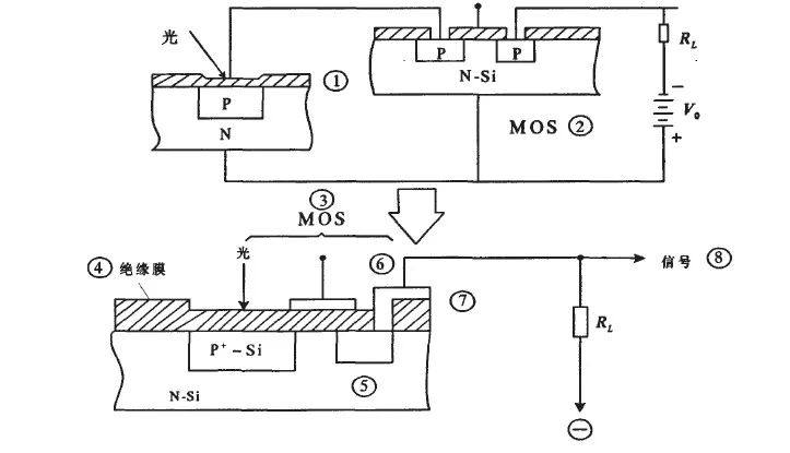
The MOS transistor and the photodiode form a structural cross-section equivalent to a pixel. During the light integration period, the MOS transistor is cut off, and the photodiode generates corresponding carriers according to the intensity of the incident light and stores them at the P-N junction of the source (position ① in the figure below).

When the integration period ends, a scan pulse is applied to the gate of the MOS transistor, turning it on, resetting the photodiode to the reference potential, and causing a video current to flow through the load, the magnitude of which corresponds to the incident light intensity.
The MOS transistor source P.N junction plays the role of photoelectric conversion and carrier storage. When a pulse signal is applied to the gate, the video signal is read out.
2. CMOS image sensor array structure
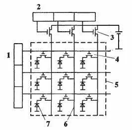
The CMOS pixel array structure consists of a horizontal shift register, a vertical shift register and a CMOS pixel array.

CMOS sensor array structure
(1-vertical shift register; 2-horizontal shift register; 3-horizontal scanning switch; 4-vertical scanning switch; 5-pixel array; 6-signal line; 7-pixel)
As mentioned above, each MOS transistor acts as a switch under the pulse drive of the horizontal and vertical scanning circuits. The horizontal shift register sequentially turns on the MOS transistors that play the horizontal scanning role from left to right, that is, the role of addressing the column, and the vertical shift register sequentially addresses the rows of the array.
Each pixel consists of a photodiode and a MOS transistor that acts as a vertical switch. The horizontal switch is turned on in sequence under the action of the pulse generated by the horizontal shift register, and the vertical switch is turned on under the action of the pulse generated by the vertical shift register, so that the reference voltage (bias) is applied to the photodiode of the pixel in sequence.

3. Working principle and process of CMOS image sensor
According to the functional block diagram of the CMOS image sensor, it can be found that the workflow of the CMOS image sensor is mainly divided into the following three steps.

Functional block diagram of a CMOS image sensor
Step 1: External light irradiates the pixel array, causing a photoelectric effect and generating corresponding charges in the pixel unit.
The scene is focused onto the image sensor array through the imaging lens. The image sensor array is a two-dimensional pixel array. Each pixel includes a photodiode. The photodiode in each pixel converts the light intensity on its array surface into an electrical signal.
Step 2: Select the pixel you want to operate through the row selection circuit and the column selection circuit, and read the electrical signal on the pixel.
During the gating process, the row selection logic unit can scan the pixel array row by row or alternately, and the same is true for the columns. The row selection logic unit and the column selection logic unit can be used together to realize the window extraction function of the image.
Step 3: Perform signal processing on the corresponding pixel units.
The image signals in the row pixel units are transmitted to the corresponding analog signal processing units and A/D converters through the signal buses of their respective columns, and converted into digital image signals for output. The main function of the analog signal processing units is to amplify the signals and improve the signal-to-noise ratio.
After the pixel electrical signal is amplified, it is sent to the correlated double sampling (CDS) circuit for processing. Correlated double sampling is an important method used by high-quality devices to eliminate some interference. Its basic principle is that the image sensor leads to two outputs, one for the real-time signal and the other for the reference signal. The same or related interference signals are removed by the difference of the two signals.
This method can reduce KTC noise, reset noise and fixed pattern noise FPN (Fixed Pattern Noise), and can also reduce 1/f noise and improve signal-to-noise ratio. In addition, it can also complete signal integration, amplification, sampling, holding and other functions.
The signal is then output to an analog/digital converter and converted into a digital signal output.
In addition, in order to obtain a practical camera of qualified quality, the chip must contain various control circuits, such as exposure time control, automatic gain control, etc. In order to make each part of the circuit in the chip move at a specified beat, multiple timing control signals must be used. In order to facilitate the application of the camera, the chip is also required to output some timing signals, such as synchronization signals, line start signals, field start signals, etc.
CMOS Image Sensor Application Fields
CMOS image sensors have the advantages of small size, low power consumption, low price and mass production, and they account for 90% of the image sensor market. They are widely used in digital cameras, smart phones, autonomous driving, security, the Internet of Things and other fields, and have huge market potential in the future.
-
digital camera
In the early days of digital cameras, most digital cameras generally used CCD imaging. However, later, CMOS developed rapidly and became an indispensable component in home SLR cameras.
Although CMOS is slightly inferior to CCD in color saturation and texture, the CMOS processing chip can make up for these, so it is still better than CCD in other aspects, such as noise reduction mechanism, fast reading speed, power saving, etc. On the market, many high-performance SLRs have the above characteristics.
-
smart phone
As we all know, mobile terminals have always been an important market for CMOS image sensors. Dual cameras and 3D cameras are widely used in smartphones, and adding lenses helps mobile phone manufacturers to widen the gap between their sales strategies and competing products. Manufacturers are more active in installing camera modules, especially using 2 million to 5 million low-pixel functional lenses to increase the number of lenses in their products.
Generally speaking, CMOS sensors can be divided into back-illuminated CMOS sensors and stacked CMOS sensors.
The back-illuminated CMOS sensor switches the photodiode and wiring layer so that light enters the photosensitive photodiode first, thereby increasing the sensitivity and significantly improving the shooting effect in low-light environments. IPhon, Xiaomi, Meizu, as we all know, are equipped with such sensors.
The stacked CMOS sensor is a derivative of the back-illuminated CMOS sensor. It is the most widely used and most advanced one in mobile phone cameras and is an exclusive technology of Sony.
-
Autopilot
Today, the automotive market has become the second largest application area for CMOS sensors after mobile phones.
With the development of autonomous driving technology, the demand for vehicle-mounted cameras has increased rapidly. Every additional camera requires an additional CMOS sensor, which directly drives the growth of the CMOS market size.
According to the latest forecast by Yole Group, the market value of CMOS image sensors has increased by US$5.5 billion from 2016 to 2022, becoming the fastest growing and highest percentage segment among automotive sensors (including various radars, sensors, etc.).
-
Security field
In the field of security monitoring, visual information needs to be obtained through cameras, which requires CMOS image sensors. In recent years, with the deep integration of the security industry with technologies such as artificial intelligence, big data, and cloud computing, the scale of the entire security monitoring market has continued to expand. Of the 851 billion yuan in total output value of China's security industry in 2020, security projects accounted for 510 billion yuan, security products accounted for 260 billion yuan, and the operation and maintenance and service market accounted for 81 billion yuan. In the future, with the further implementation of the security industry infrastructure, the scale of the CIS market in the security monitoring field will continue to grow.
-
IOT (Internet of Things) Field
In the field of IOT, a large number of electronic hardware devices need to be equipped with camera modules to realize image, face recognition, video calls and other functions. Such as TV, smart speakers, drones, VR/AR and other products. In addition, a large number of CMOS image sensors are also needed in medical and industrial systems. Now the medical and scientific research fields are seeking to use lower-cost and better-effective CMOS sensors to replace most old products; with the development of machine vision, more and more industrial production lines will introduce image sensors to improve production efficiency and quality.
Canon CMOS Image Sensor Selection
Canon CMOS Image Sensor Product List


High resolution products

Machine Vision/Monitoring Product Series

·END·


